Interchip Connectivity: C2C, MIPI LLI and the path to 3D IC and TSV
, 2012年02月23日
C2C and LLI: The first standards created with the “combo chip” in mind
As you may already know, the purposes of the chip-to-chip (C2C) interface an d the MIPI Low Level Interface (MIPI LLI) are essentially the same: Hook two separate SoCs together in such a manner that they work together as one chip.
The most obvious use case for these two standards is to enable a mobile phone’s modem baseband chip to connect to an application processor and share its DRAM through the very low latency connection. The value proposition of this is a no-brainer, because the phone vendor no longer has to have a dedicated DRAM connected to the modem baseband. This saves about $2, as well as some PCB board space.
The inspiration for these standards was to allow designers to create a virtual “combo chip” combining the best applications processor SoC and best modem baseband SoC to meet a phone’s requirements. However, there is so much more that can be done using these types of interchip interfaces. For instance, modem vendors are using these standards to create a base modem “platform” SoC which can then be extended by additional coprocessor chips to add new features such as LTE.
Imagine what can be done with this type of architecture: Do you need to respond quickly to changes in phone video requirements but not sure how market demand will change over time? Then create a “mother” SoC with separate video companion chips meeting different market segments. Want to have the same platform that meets DTV and STB requirements? Then create a mother SoC with separate companion chips having different interfaces, encoders and decoders. The benefits of this architecture flexibility increase when a common software platform is reused for the various virtual combo chips.
“Combo chips” will change how we design SoCs
Let’s assume you think that everything I described above is not just fantasy. Then your next reaction is probably, “But this will change how we design and partition hardware and software…”
And you are correct.
To get the most economic advantage from this combo chip approach, designers will have to spend more time up front partitioning the hardware and software and determining how tightly the separate dies within the combo chip are coupled. At one extreme, the two chips could be loosely coupled, with the companion chip perhaps only sharing a block of memory allocated by the mother chip. Or in contrast, the two chips could be tightly coupled such that the system’s initiators and targets are spread across both chips.
A key factor is that this type of design approach will require hardware designers and software coders to work together more closely and much sooner in the design process to create a base “platform” that can be used with multiple companion chips in an economically viable manner.
The path to 3D IC
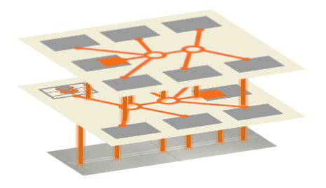
What does this have to do with 3D IC? A lot of the press and commentary today about 3D IC and TSV revolves around manufacturing and business model issues, but fails to address how system architectures and design processes will have to change to take advantage of these opportunities. The first sandbox where new ideas will be tried, polished and perfected is in today’s “combo chip” arena.
So if you want a glimpse of what creative engineers will be able to do when 3D IC silicon and TSV are available, then keep an eye on the people using C2C and MIPI LLI today.
Learn more about chip-to-chp (C2C) and MIPI LLI interchip connectivity:
- Visit the Arteris website C2C pages
- How to choose between C2C and MIPI LLI: “MIPI LLI or C2C?”
